P-Sort Semiconductors
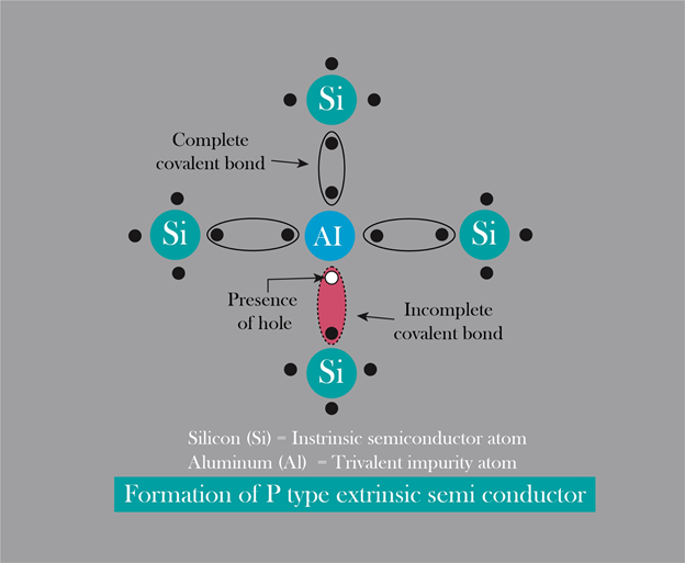
P-type semiconductors are components of a gaggle Ⅳ equivalent to Silicon (Si) or Germanium (Ge) which are doped with components of the group Ⅲ that are generally known as trivalent impurities equivalent to Boron (B) or Aluminum (Al). In different phrases, we will say that an impurity is added to pure semiconductors to make P-type semiconductors. They’ve an additional gap or constructive cost on them as a result of the outermost shell has an unpaired electron.
N-Sort Semiconductors
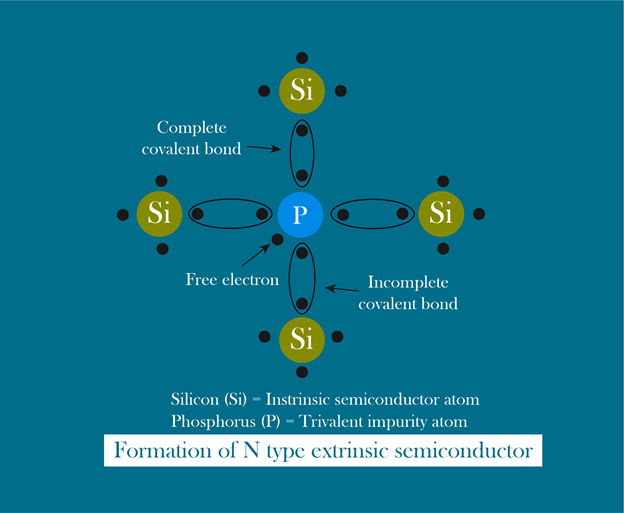
N-type semiconductors are components of a gaggle Ⅳ equivalent to Silicon (Si) or Germanium (Ge) which are doped with components of the group Ⅴ also referred to as pentavalent impurities equivalent to Phosphorus (P) or Antimony (Sb). Any such semiconductor has an additional electron or unfavourable cost on them as a result of the outermost orbit of Silicon or Germanium will get an additional electron when it’s doped with group Ⅴ components.
Development of PN Junction Diode
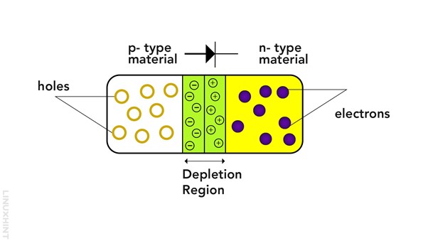
When a P-type and N-type semiconductor materials are mixed, a junction is shaped between them that is named a PN junction. Throughout the formation of a PN junction, electrons from N-type materials attempt to drift in the direction of holes in P-type materials, and holes from P-type materials transfer in the direction of electrons in N-type materials. This leads to the formation of a depletion area between P-type and N-type materials that acts as a possible barrier for the stream of present.
So, the PN junction turns into a two-terminal semiconductor machine that both permits present to stream from it or blocks present. In P-type materials, holes are the bulk of cost carriers, and in N-type materials, free electrons are the bulk of cost carriers.
Ahead Biased Situation of PN Junction Diode
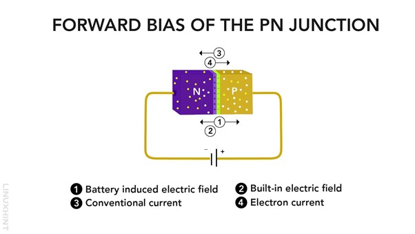
Within the forward-biased situation of a PN junction diode, it behaves as a conductor and permits present to stream by way of it. The connections are made such that the constructive terminal of the battery is built-in with the P-type materials and the N-type materials is built-in with the unfavourable terminal of the battery.
The utilized voltage have to be larger than the potential barrier of the diode. For instance, the Si diode has a possible barrier of 0.7V and the Germanium diode has a possible barrier of 0.3V. When ahead voltage is utilized to the PN junction, the electrical subject of the depletion area is reverse to the electrical subject utilized by the battery.
When each electrical fields add up, the ensuing electrical subject is much less in magnitude than each. So, the least resistance is obtainable to the stream of present and the diode conducts present.
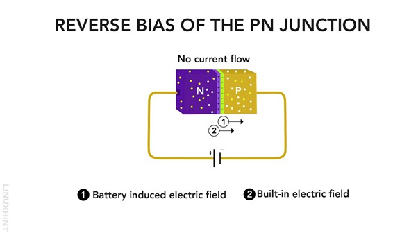
Reverse Biased Situation of PN Junction Diode
Within the reverse biased situation of the PN junction diode, it behaves as an insulator and doesn’t enable present to stream by way of it. The connections are made such that the constructive terminal of the battery is built-in with N-type materials and the P-type materials is built-in with the unfavourable terminal of the battery.
When a reverse voltage is utilized to the PN junction, the electrical subject of the depletion area is in the identical path as the electrical subject utilized by the battery.
When each electrical fields add up, the ensuing electrical subject is bigger in magnitude than each, and a really thick depletion area is shaped. So, a big resistance is obtainable to the stream of present and the diode doesn’t conduct present. If the reverse voltage could be very giant in magnitude, it might trigger the diode to interrupt down in reverse situation and conduct indefinitely.
I-V Traits for Semiconductor Diodes
The I-V traits of semiconductor diodes clarify the currents and voltages of PN junctions in ahead and reverse-biased situations. Within the I-V traits graph, voltage is taken alongside the x-axis and present is taken alongside the y-axis.
Because the graph under signifies, in a forward-biased situation when voltage is utilized to the PN junction, the diode begins conducting slowly. After a while, when the diode totally overcomes the potential barrier, it begins conducting fully. At the moment, the present by way of the diode will increase quickly on the identical voltage utilized.
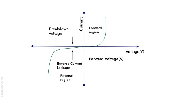
Nonetheless, in reverse-biased situations, when a reverse voltage is utilized to the PN junction, it doesn’t conduct present. Nonetheless, a small reverse leakage present flows as a result of minority cost carriers current in P-type and N-type materials. This present stream as a result of holes are attracted by the unfavourable aspect and electrons are attracted by the constructive aspect of the battery. These minority cost carriers sweep throughout the depletion area and trigger reverse leakage present.
Reverse Breakdown Voltage
Within the reverse situation, if the utilized reverse voltage could be very giant such that it overcomes the thick depletion area, it causes the diode to break down. On this situation, present surges by way of the diode are noticed, and it begins conducting. The voltage past which a diode breaks down is named the breakdown voltage.
Functions of PN Junction Diode
Diodes are the fundamental constructing block of modern-day electronics. PN junction diodes are largely used as Gentle Emitting Diodes (LEDs) and photodiodes. Moreover, they’re additionally utilized in photo voltaic cells, rectifiers, clippers, clampers, logic gates, management circuits, and voltage-controlled oscillators.
Conclusion
PN junction semiconductor diodes are easy units made by way of the mixture of P-type and N-type supplies. These supplies are created by doping of trivalent or pentavalent components of group Ⅲ and group Ⅴ in pure semiconductors. Diodes can behave as conductors in addition to insulators in ahead and reverse-biased situations, respectively. In addition they have quite a few functions within the subject of contemporary electronics.