
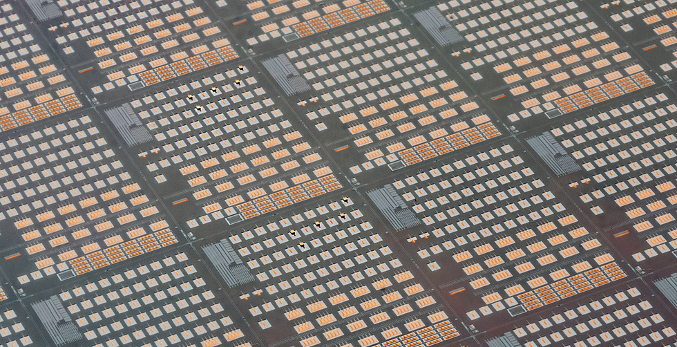
Photonic built-in circuits, which mix a set of optoelectronic features on a single chip, are an more and more widespread a part of on a regular basis life. They’re utilized in high-speed optical transceivers that hyperlink server racks in knowledge facilities, together with the one used to ship the IEEE Spectrum web site, in lidars to maintain self-driving automobiles on monitor, and in spectrometers to identify chemical compounds within the environment, amongst many different purposes. All these programs have grown cheaper and, in some instances have change into economically possible, by making many of the IC with silicon fabrication applied sciences.
Engineers have been capable of combine almost each necessary optical perform, together with the necessities of modulation and detection, on silicon photonic chips, aside from one: mild emission. Silicon itself doesn’t try this effectively, so semiconductors manufactured from so-called III-V supplies, named for the place of their constituents on the periodic desk, are usually used to make individually packaged parts to supply mild.
In the event you can dwell with an exterior laser diode in your design, there’s no situation. However a number of elements have just lately been pushing engineers to combine lasers with silicon photonics. There could also be, for instance, no house for a separate mild supply. Tiny gadgets meant to be implanted within the physique to watch, for instance, blood-sugar ranges, may face this downside. Or an utility’s value may name for nearer integration: When you may match a whole bunch or hundreds of lasers on a single silicon wafer, you’ll find yourself with a decrease value and infrequently larger reliability than when you have to join separate chips.
There are lots of methods to attain this tighter integration of lasers and silicon. Working at Imec, a Belgium-based nanoelectronics R&D heart, we’re at present pursuing 4 primary methods: flip-chip processing, microtransfer printing, wafer bonding, and monolithic integration. What follows is a information to how these approaches work, their degree of scalability and maturity, and their execs and cons.
![]() In flip-chip bonding, laser dies [left] are individually transferred and bonded to a silicon photonics wafer.Emily Cooper
In flip-chip bonding, laser dies [left] are individually transferred and bonded to a silicon photonics wafer.Emily Cooper
Flip-Chip Integration
A simple manner of immediately integrating lasers on silicon wafers is a chip-packaging know-how referred to as flip-chip processing, which could be very a lot what it appears like.
A chip’s electrical connections are on prime the place the uppermost layer of interconnects terminate on metallic pads. Flip-chip know-how depends on balls of solder hooked up to these pads. The chip is then flipped over so the solder traces up with corresponding pads on the chip’s bundle (or in our case onto one other chip). The solder is then melted, bonding the chip to the bundle.
The idea is analogous however extra exacting when making an attempt to bond a laser chip to a silicon-photonics chip. Edge-emitting lasers are totally processed on a wafer, diced into particular person chips, and examined by the seller. The person laser chips are then bonded to the goal silicon photonic wafer, utilizing a high-precision model of the flip-chip course of, one laser die at a time. The tough half is making certain that the output of the laser, which emits on the edge, traces up with the enter of the silicon photonics chip. We use a course of referred to as butt-coupling, the place the laser is positioned in a recessed a part of the silicon, so it’s laterally abutted to the etched side of a silicon photonics waveguide.
For this to work, the flip-chip course of requires submicrometer alignment precision in all three dimensions. Specialised flip-chip bonding instruments have been developed over the previous a number of years to do the job, and we and our collaborators and improvement companions have used them to optimize the meeting processes. Leveraging a sophisticated pick-and-place instrument that makes use of machine imaginative and prescient to take care of exact alignment, we will place and bond laser gadgets with precisions higher than 500 nanometers in just some tens of seconds.
In 2021, we additionally established a wafer-scale silicon-photonics course of that improves on this efficiency. It provides mechanical alignment pedestals and a extra exactly etched butt-coupling interface to the silicon chip to attain vertical alignment of higher than a couple of hundred nanometers. Utilizing these strategies, we assembled sure laser gadgets on a 300-millimeter silicon photonics wafer. We had been delighted to see that as a lot as 80 p.c of the 50 milliwatts of laser mild from every system was coupled into the silicon photonics chip to which it was hooked up. Within the worst instances, the coupling was nonetheless round 60 p.c throughout the entire wafer. These outcomes rival the form of coupling efficiencies achieved with energetic alignment, a extra time-consuming course of the place mild from the laser itself is used to steer the alignment course of.
A big benefit of the flip-chip method is simplicity and suppleness within the form of chips that get mated. As a result of they are often produced in current fabrications traces with restricted further engineering, they will every be sourced from a number of producers. And, with rising market demand, flip-chip meeting providers are being provided by a rising variety of distributors. Then again, the sequential nature of the method—every laser die must be picked up and positioned individually—is a major disadvantage. It limits the manufacturing throughput and the potential for deep value reductions in the long term. That’s particularly necessary for cost-sensitive purposes, like client merchandise, and for programs that require a number of laser gadgets per chip.
 Laser dies are hooked up to silicon photonics chips utilizing a high-precision model of the flip-chip methodology. Optoelectronics
Microtransfer Printing
Microtransfer printing removes among the alignment difficulties of butt-coupling, whereas additionally making the meeting course of quicker. Simply as in flip-chip processing, the light-emitting gadgets are grown on III-V semiconductor substrates. However there’s an enormous a distinction: The III-V wafers aren’t diced into particular person chips. As a substitute, the lasers on the wafer are undercut in order that they’re hooked up to the supply wafer solely by small tethers. The gadgets are then picked up all along with a instrument that’s like an ink stamp, breaking the tethers. The stamp then aligns the lasers with waveguide constructions on the silicon photonics wafer and bonds them there.
Whereas flip-chip know-how makes use of metallic solder bumps, microtransfer printing makes use of an adhesive or may even make do with simply molecular bonding, which depends on the Van der Waals forces between two flat surfaces, to carry the laser in place. Additionally, the optical coupling between the sunshine supply and the waveguide within the silicon photonics chip occurs by means of a distinct course of. Referred to as evanescent coupling, the method locations the laser on prime of the silicon waveguide constructions and the sunshine “bleeds” into it. Though much less energy is transferred this manner, evanescent coupling calls for much less exact alignment than does butt-coupling.
Having higher tolerance in alignment allows this system to switch hundreds of gadgets directly. So it ought to, in precept, permit for larger throughput than flip-chip processing and be supreme for purposes that ask for the mixing of huge numbers of III-V parts per unit space.
Though switch printing is a longtime course of for making microLED shows, resembling these wanted for a lot of augmented actuality and digital actuality merchandise, shouldn’t be but prepared for printing lasers or optical amplifiers. However we’re getting there.
Final yr, Imec succeeded in utilizing switch printing to connect such mild sources onto a wafer containing silicon-photonic waveguides, high-speed optical modulators, and photodetectors. We’ve additionally printed infrared lasers tunable over 45 nm of wavelength and high-pulse power gadgets appropriate for chip-based spectroscopy programs. These had been made just for demonstration functions, however we see no basic cause that this method can’t obtain good outcomes with excessive yields. So we count on the know-how to be prepared for deployment on manufacturing traces inside a couple of years.
![]() In microtransfer printing, laser dies [red rectangles, left] are weakly held in place on their very own wafer. A stamp [light grey] picks a number of lasers up directly and locations them on the silicon photonics wafer. Emily Cooper
In microtransfer printing, laser dies [red rectangles, left] are weakly held in place on their very own wafer. A stamp [light grey] picks a number of lasers up directly and locations them on the silicon photonics wafer. Emily Cooper
Die-to-Wafer Bonding
Exactly aligning light-emitting parts with their silicon-photonics mates is the vital step within the two applied sciences we mentioned. However one approach, a type of what’s referred to as III-V-to-silicon-wafer bonding, finds a manner round that. As a substitute of transferring already-constructed lasers (or different light-emitting parts) to a processed silicon wafer, this scheme bonds clean dies (and even small wafers) of a III-V semiconductor to that silicon wafer. You then construct the laser gadgets you want on prime of the place the corresponding silicon waveguides already are.
Of the transferred materials, we’re solely focused on that skinny stratum of crystalline III-V materials, referred to as the epitaxial layers. So after bonding with the silicon wafer, the remainder of the fabric is eliminated. Laser diodes could be fabricated within the epitaxial layers aligned to underlying silicon waveguides utilizing normal lithographic and wafer-scale processing. Any unneeded III-V supplies is then etched away.
Engineers at Intel developed this method prior to now decade, and the primary business merchandise constructed with it, optical transceivers, had been launched in 2016. The tactic permits excessive throughput integration, as a result of it allows parallel processing of many gadgets directly. Like switch printing, it makes use of evanescent coupling between the III-V and silicon supplies, yielding an environment friendly optical interface.
One disadvantage of III-V-to-silicon-wafer bonding is that you simply want substantial funding to ascertain a producing line that may deal with the III-V processing steps utilizing instruments meant for fabricating silicon wafers, that are both 200-mm or 300-mm diameter. Such instruments are very completely different from these utilized in a laser-diode foundry, the place the everyday wafer diameter is significantly smaller.
![]() In die-to-wafer bonding, clean items of III-V semiconductor [pink] are bonded to an already-processed silicon photonics wafer. The III-V materials is processed into lasers above the silicon waveguides. The remainder of the III-V materials is then etched away.Emily Cooper
In die-to-wafer bonding, clean items of III-V semiconductor [pink] are bonded to an already-processed silicon photonics wafer. The III-V materials is processed into lasers above the silicon waveguides. The remainder of the III-V materials is then etched away.Emily Cooper
Monolithic Integration
The best method to mating the 2 completely different supplies concerned could be to develop III-V semiconductors immediately on silicon, an method referred to as monolithic integration. This might put off any want for bonding or alignment, and it will cut back the quantity of III-V materials that’s wasted. However many technological hurdles should be overcome for this tactic to be sensible. So analysis towards this objective continues at Imec and elsewhere.
The principle purpose of that analysis is to create crystalline III-V supplies with a low density of defects. The elemental downside is that there’s fairly a mismatch—greater than 4 p.c—between the lattice spacing of atoms in silicon and that of the atoms within the III-V semiconductors of curiosity.
Due to this lattice mismatch, each III-V layer grown on the silicon turns into strained. After only some nanometers of III-V movie is added, defects within the crystal emerge, releasing the built-up pressure. These “misfit” defects type alongside traces that penetrate the complete III-V layer. These defects embody traces of open crystal bonds and localized crystal distortion, each of which severely degrade the efficiency of optoelectronic gadgets.
To forestall these defects from killing the laser, they should be confined to locations removed from the system. Doing that typically includes laying down a layer of III-V materials that’s a number of micrometers thick, forming a hefty buffer between the misfit defects beneath and a strain-free area above, the place the laser gadgets could be fabricated. Researchers at College of California, Santa Barbara, have reported glorious progress utilizing this method, demonstrating high-efficiency gallium-arsenide-based quantum-dot lasers with promising reliability lifetimes.
These experiments have been accomplished solely at small scales, nonetheless. Extending the approach to the 200- or 300-mm wafers utilized in trade will likely be tough. The addition of thick buffer layers might result in varied mechanical issues, resembling cracks growing contained in the III-V movie or the wafer bowing. As well as, with the energetic system on prime of such a thick buffer layer, it’s difficult to couple mild to an underlying waveguide within the silicon substrate.
To bypass these challenges, Imec has launched a brand new method to monolithic integration referred to as nanoridge engineering, or NRE. The approach goals to power defects to type in such a confined house that working gadgets could be constructed little greater than 100 nm above the interface with the underlying silicon.
NRE confines the defects to small areas utilizing a phenomenon referred to as aspect-ratio trapping. It begins by creating slim and deep trenches inside a layer of silicon dioxide insulator. On the backside of the ditch, the place the insulator meets the silicon, a groove cuts into the silicon, giving the void an arrowhead-shaped cross part. A skinny layer of III-V crystal is then grown inside the trench, and the strain-induced misfit defects are effectively trapped on the trench sidewalls, stopping these traces of defects from penetrating farther. After the ditch is crammed, the expansion continues to type a bigger nanoridge of III-V materials above the ditch. The fabric in that nanometer-scale ridge is sufficiently freed from defects in order that it may be used for laser gadgets.
Most analysis on monolithic integration is finished on the degree of enhancing particular person gadgets and figuring out causes for his or her failure. However Imec has already made substantial progress in demonstrating full wafer-scale integration with this system, producing high-quality GaAs-based photodiodes in a 300-mm silicon pilot line. The following milestone would be the demonstration of an electrically pumped laser based mostly on the same design to the photodiodes. Nanoridge engineering continues to be beneath improvement within the lab, but when it really works, it is going to little question have a big influence on this trade.
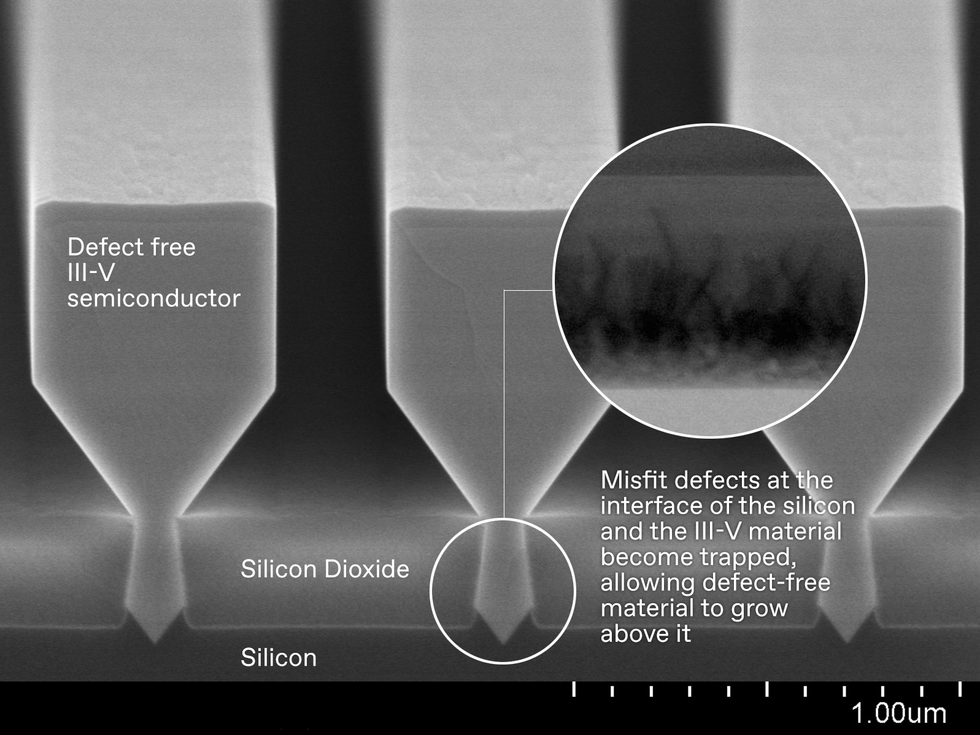 Nanoridge engineering grows laser-suitable semiconductor in specially-shaped trenches within the silicon. The form of the ditch traps defects [inset] effectively beneath the world the place the laser is constructed.imec
The Outlook for Lasers on Silicon
Within the subsequent few years, every of the approaches mentioned right here will certainly progress additional. We count on that they may ultimately coexist to serve completely different utility wants and use instances.
The comparatively modest setup value and readiness of flip-chip laser meeting will allow near-term merchandise and is especially engaging for purposes requiring just one or a few lasers per photonic IC, such because the optical transceivers utilized in knowledge facilities. As well as, the pliability inherent on this method makes it engaging for purposes that require nonstandard laser wavelengths or unusual photonics know-how.
For prime-volume purposes that require a number of lasers or amplifiers per photonic IC, switch printing and die-to-wafer bonding provide larger manufacturing throughput, smaller coupling losses, and the potential for deeper value reductions. As a result of the setup prices listed here are considerably larger, the purposes for which these strategies are appropriate should have massive markets.
Lastly, direct III-V epitaxy on silicon, such because the NRE approach, represents the final word degree of laser integration. However we and different researchers should make additional progress in materials high quality and wafer-scale integration to unlock its potential.
The authors want to thank Katrien Mols.
From Your Web site Articles
Associated Articles Across the Net